
About Us
Petasemi is a private company invested by a team of leaders of optical communication industry, focusing on high speed, wide power range, supreme sensitivity, market leading reliability InP & GaAs optoelectronic chips development & mass production with the best in class manufacturing facility.
We provide excellent performance, high quality chip for the fields of optical communication, sensor, medical and display applications. Our engineers have 20+ years R&D experience on LD, PD chips and well recognized as the best experts in Asia, with billion chips successful mass production record.
Independent & Complete Fab
- 6000 sq.m fab
- 4000 sq.m cleanroom
- 300+ equipment & instruments
Experienced & Dynamic Team
- 60+ skillful staff
- 20+ professional engineers
- 20+ years experience
Product Key Techniques
- High end optical chip design
- High quality material epitaxy
- Precise micro-structure fabrication
- Reliable passivation & coating
- Failure mechanism analysis
Safeguard Mechanism
- Product safety and environmental protection standards
- Full process quality control
- Internal risk management
Technology
Petasemi is a leading designer and manufacturer, providing an innovative, cost-effective, and lower-power consumption solution of optical and photonic products.
With key technologies of design, process, monitor, test and mass production management, we provide versatile design, reliable manufacture, stable production and superior performance.
- CrossLight
- Pics3D
- Lastip
- Ansoft
The Fab
Petasemi established a full scale state-of-the-art III-V fab enabling us to have full control from design to wafer growth, processing, and testing.
- 3inch chip line(upgrade to 4inch later).
- 6000 sq.m fab
- 4000 sq.m, clean room, J5~J8.
- 300+ equipment & instrument from material epitaxy to wafer process to chip test.
- 15,000 pieces of wafers, 150 millions pieces of chips Annual output.
Products
Petasemi is an industry leading designer and manufacturer. With key technologies of design, process, test and mass production management, providing an innovative, cost-effective, and lower-power consumption solution of optical and photonic products.
Petasemi offers GaAs and InGaAs based photodetectors, both PIN PD and APD are available. The product response wavelength covers 850nm and 1100nm ~ 1700nm, which has the characteristics of low dark current, high responsivity, and high reliability.
Application scenarios include telecommunications, data center , monitoring and sensing, Active Optical Cable (AOC), long wavelength LiDAR, quantum communication and microwave photonic links.
- 850nm,1100nm~1700nm
- MPD, PIN, APD, TWPD, UTC
- 10G/25G/50G/HP/GM
- PON, Wireless, Datacenter, Sensor
| Product Model | Wavelength | Product Description |
|---|---|---|
| HC-PD-1000 | 1310nm/1550nm | Monitor PD |
| HC-PD-200 | 1310nm/1550nm | Monitor PD |
| HC-EMPD-100 | 1310nm/1550nm | Edge-Illuminated Monitor PD |
| HC-PD-70 | 1310nm/1550nm | 2.5Gbps PD |
| HC-PD-45 | 1310nm/1550nm | 10Gbps PD |
| HC-PD-20 | 1310nm | 25GBaud PD |
| HC-PD-20A1 | 1310nm | 4×25GBaud PD Array |
| HC-PD-16 | 1310nm | 56GBaud PD |
| HC-PD-16A1 | 1310nm | 4×56GBaud PD Array |
| HC-PD-16A2 | 1310nm | 4×56GBaud PD Array |
| HC-PD-16A3 | 1310nm | 8×56GBaud PD Array |
| HC-PD-16A4 | 1310nm | 8×56GBaud PD Array |
| HC-PD-10 | 1310nm | 112GBaud PD |
| HC-GPD-40 | 850nm | 25GBaud PD |
| HC-GPD-40A1 | 850nm | 4×25GBaud PD Array |
| HC-SPD-32A1 | 850nm | 4×56GBaud PD Array |
| HC-APD-30 | 1310nm/1550nm | 2.5Gbps Avalanche PD |
Petasemi relies on its unique InP based photon integration technology platform, with years of technolog accumulation in high end optical communication chip, strong product portfolio, and high speed and high reliability design with complete and independent intellectual property rights, making it an important resource for high end optical chips in China.
EOPTERA has launched mature 2.5G-25G full series of DML, high power DFB laser for silicon optical communication and so on. The application scenarios include data centers, telecommunication backbone networks, wireless medium/forward transmission, and broadband access optical networks.
- 1270nm, 1310nm, 1490nm, 1550nm, 1577nm
- SMFP, MMFP, DFB, EML
- 2.5G/10G/25G/CW
- PON, Wireless, Datacenter, Sensor
| Product Model | Wavelength | Power | Product Description |
|---|---|---|---|
| HC-1310FP-A | 1310nm | 5~10mW | 2.5Gbps |
| HC-1550FP-A | 1550nm | 5~10mW | 2.5Gbps |
| HC-1310FP-I | 1310nm | 5~10mW | 10Gbps |
| HC-1270DFB-A | 1270nm | 5~10mW | 2.5Gbps |
| HC-1310DFB-A | 1310nm | 5~10mW | 2.5Gbps |
| HC-1490DFB-A | 1490nm | 5~10mW | 2.5Gbps |
| HC-1550DFB-A | 1550nm | 5~10mW | 2.5Gbps |
| HC-1270DFB-I | 1270nm | 5~10mW | 10Gbps |
| HC-1310DFB-I | 1310nm | 5~10mW | 10Gbps |
| HC-1310DFB-E | 1310nm | 5~10mW | 25Gbps |
| HC-1310DFB-F | 1310nm | 70mW | CW |
| HC-1310DFB-F1 | 1310nm | 100mW | CW |
| HC-1310DFB-F2 | 1310nm | 200mW | CW |
| HC-1550DFB-F | 1550nm | 100mW | CW |
Petasemi offers GaAs and InP based high-power edge emitting laser diode chips. It has a portfolio of continuous, quasi continuous, and pulse product series, with wavelength range of 780nm-1700nm, which has the characteristics of good wavelength consistency, high power density, and high reliability.
The product is mainly used in the fields of solid-state or fiber laser pump sources, and light sources for LiDAR, robot vacuum cleaners, and service robot.
- 808nm/905nm/974nm/1060nm/1550nm
- SMFP, MMFP, FP Bar, DFB
- 100mW~1000W
- Sensor, Medical, Display
| Product Model | Wavelength | Power | Product Description |
|---|---|---|---|
| HC-808FP-CW50W | 808nm | 50W | Pumping of solid-state lasers, medical systems |
| HC-808FP-CW100W | 808nm | 100W | Pumping of solid-state lasers, medical systems |
| HC-808FP-QCW300W | 808nm | 300W | Pumping of solid-state lasers, medical systems |
| HC-1310FP-CW01W | 1310nm | 100mW | Telecommunication |
| HC-1550FP-CW01W | 1550nm | 100mW | Telecommunication |
| HC-905FP-PW40W | 905nm | 40W | Range finding, LiDAR applications |
| HC-905FP-PW90W | 905nm | 90W | Range finding, LiDAR applications |
| HC-905FP-PW120W | 905nm | 120W | Range finding, LiDAR applications |
| HC-905FP-PW150W | 905nm | 150W | Range finding, LiDAR applications |
| HC-905FP-PW200W | 905nm | 200W | Range finding, LiDAR applications |
| HC-905FP-PW300W | 905nm | 300W | Range finding, LiDAR applications |
Contacts
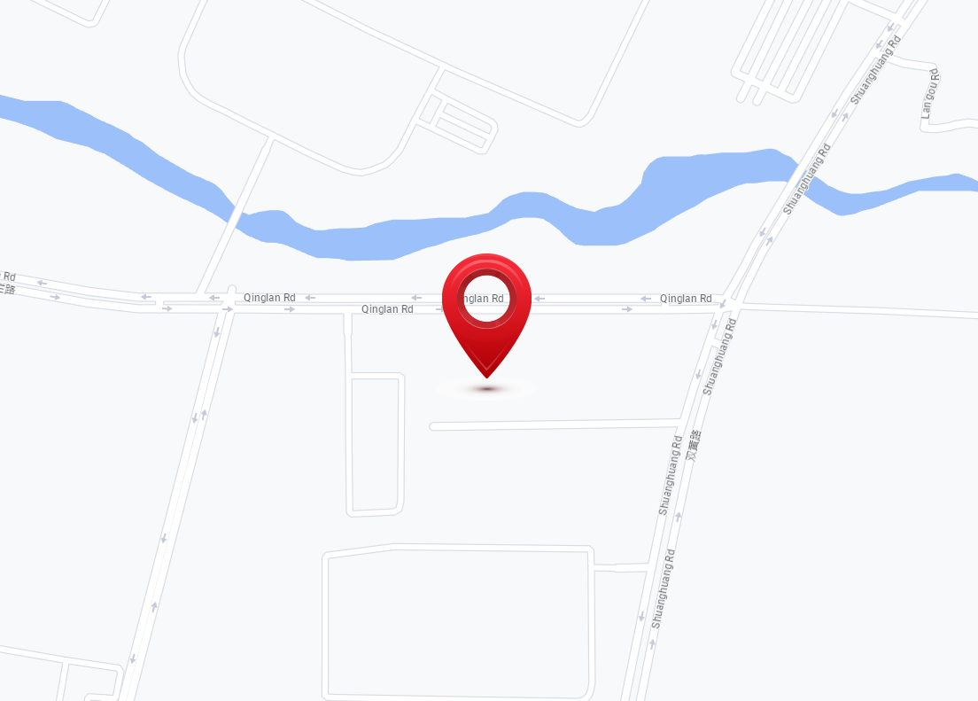
Address: Building 2, No.1443, Qinglan Road, Southwest Airport Economic Development Zone, Shuangliu District, Chengdu
Email:
Business inquiries: sales@petasemi.com
Join us: talent@petasemi.com
Phone: 0086-28-85823016
Copyright © 2024 Petasemi. All rights reserved.